
Instant Quote Request
All About the PCB Silkscreen Process
With over 20 years in PCB manufacturing, we know what it takes to build boards that work —
including the often-overlooked silkscreen layer.
At PCB Traces Inc., we manufacture silkscreened PCBs to your exact specifications.
Whether you need reference designators, logos, test points, or component outlines,
we put quality — and your requirements — first.
What Is PCB Silkscreen?
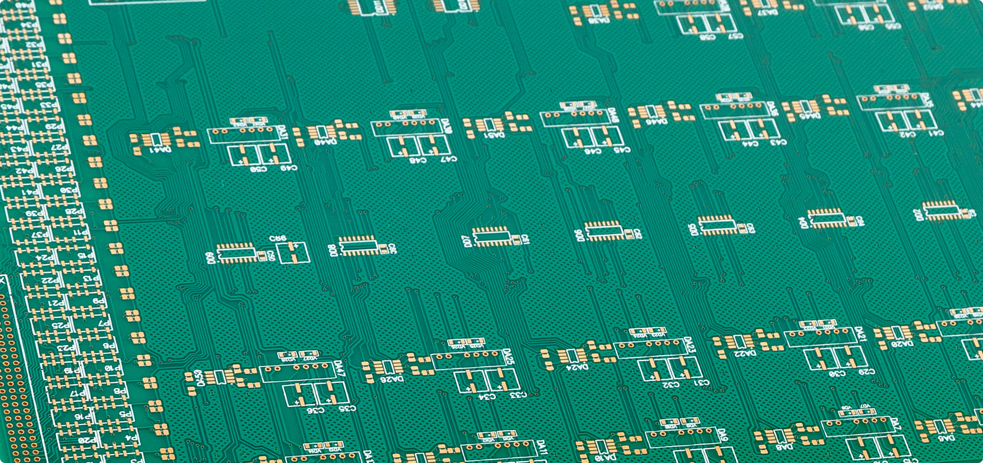
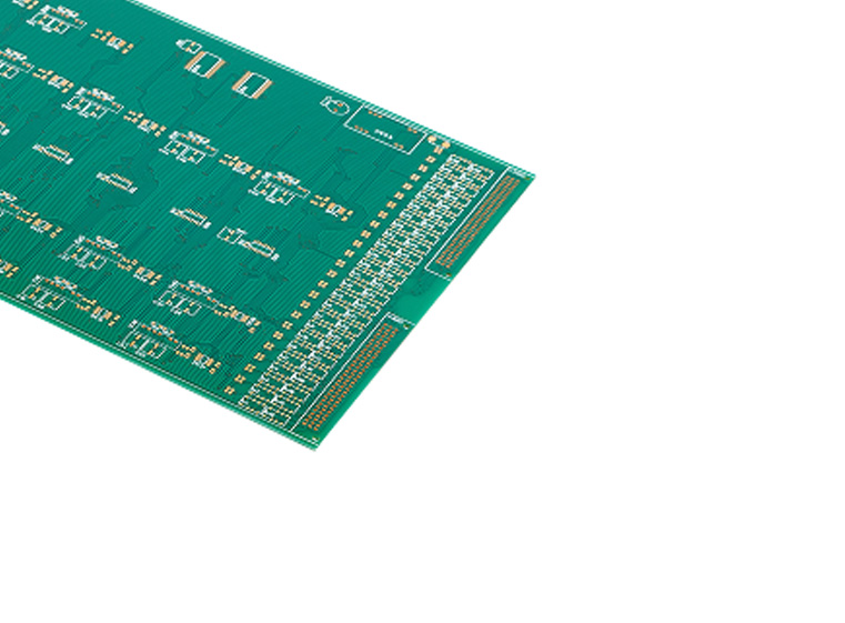
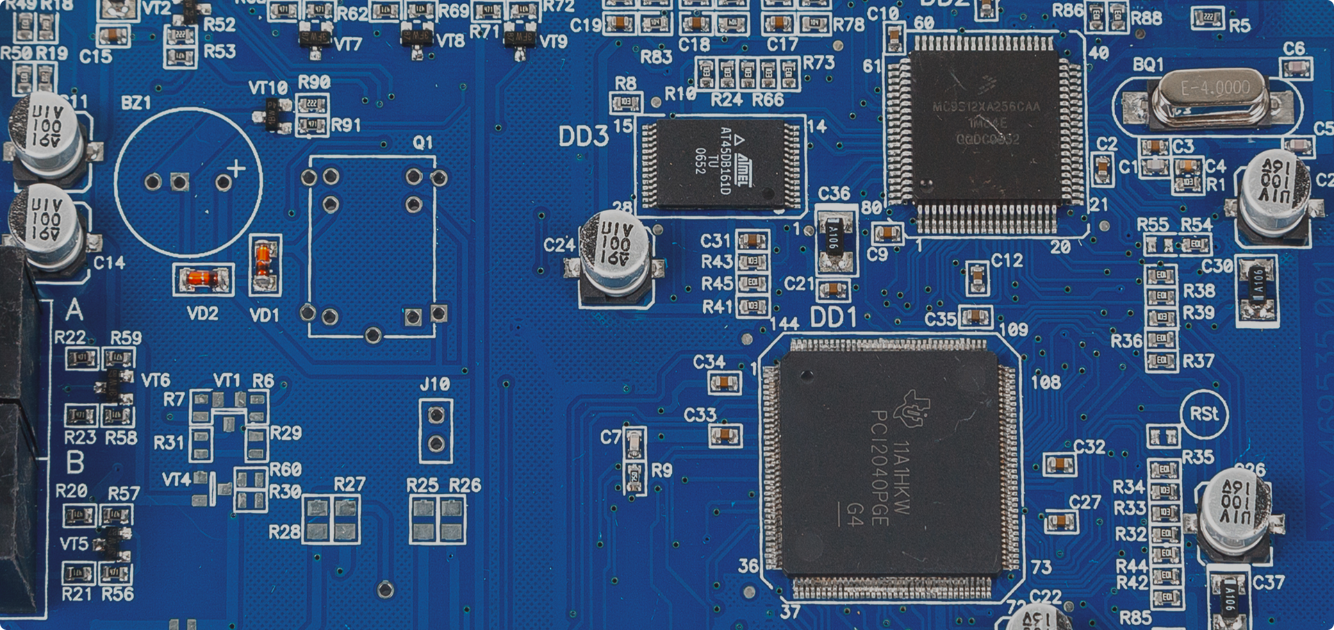
Silkscreen is a layer of non-conductive epoxy ink traces applied to the board. It typically shows:
- Component references (R1, C2, U3)
- Test points
- Logos, marks, and symbols
- Polarity and pin-1 indicators
Silkscreen is most often applied to the component side, but can also be used on the solder side.
While adding a second side may increase cost slightly, it makes assembly, testing, and rework much easier.
Ink colors — white, black, and yellow are standard. Other colors available on request.
The 3 Common Silkscreen Methods
We use direct legend printing and LPI for most orders — cleaner results, better adhesion, and faster turnaround.
The Silkscreen Process at PCB Trace
We break silkscreen into six practical stages:
- Design Review – We check your CAD files for legibility, clearance, and manufacturability;
- Board Preparation – Cleaning and surface treatment to ensure ink adhesion;
- Printing – Ink is applied using the method best suited to your design;
- Handling & Alignment – Precise registration to avoid misprints;
- Inspection – Automated and visual checks for missing or blurry markings;
- Curing & Final QC – UV or thermal cure, then one last inspection before shipping.
Why Silkscreen Quality Matters
A poor silkscreen — wrong polarity marks, smeared text, missing references — can cause assembly errors, rework, and delays.
At PCB Trace, we treat silkscreen as part of the board, not an afterthought. Every board we ship is clearly marked,
easy to assemble, and built to your specs.
Stay ahead in the dynamic world of PCBs —
trends and insights delivered to you
Understanding AOI and Its Critical Role in PCB Assembly
Understanding AOI and Its Critical Role in PCB Assembly
Understanding AOI and Its Critical Role in PCB Assembly
Get Your Free DFM Checklist
Catch design errors before fabrication.
Enter your email to download